Lets Dive into Modern Computing Architecture
The Atomic Foundation: Bits, Bytes, and the Binary Language
To understand the power of a modern supercomputer, one must first look at the “atom” of the digital world: the Bit. A bit (binary digit) is the simplest form of information, representing a logical state of 1 or 0. In the physical realm of hardware, this is a transistor acting as a gate—either allowing electricity to flow or blocking it.
When we group eight of these bits together, we create a Byte. This eight-bit architecture was not an arbitrary choice. It provides 256 unique combinations, exactly enough to map the entire English alphabet (both upper and lower case), numbers, and essential control characters into the original ASCII standard.
Today, the confusion between bits and bytes remains the most common hurdle for consumers. Networking is measured in bits (megabits per second, or Mbps) because telecommunications care about the “flow” of individual pulses. Storage, however, is measured in Bytes (Gigabytes or Terabytes) because computers care about the “volume” of completed data packets. This 8:1 ratio is the reason a “1,000 Mbps” fiber connection actually downloads a file at roughly 125 MB/s.
The Evolution of “Word Size”: 8-bit to 128-bit
The history of computing is a story of expanding “word size”—the maximum number of bits a CPU can process in a single internal register.
1. The Retro Era (8-bit & 16-bit)
In the late 1970s, 8-bit microprocessors like the MOS 6502 defined the “Home Computer Revolution.” These chips could only “see” memory addresses, limiting them to a mere 64 KB of RAM. By the early 80s, 16-bit chips like the Intel 8086 arrived. With a 20-bit address bus, they broke the 64 KB barrier, allowing for 1 MB of RAM—a staggering amount for the time.
2. The 32-bit Era and the 4 GB Wall
The 32-bit era (symbolized by the Intel 80386) brought us into the modern age of graphical interfaces. However, it introduced a hard physical limit: a 32-bit register can only point to 4,294,967,296 unique memory locations. This created the 4 GB RAM Wall. No matter how much RAM you plugged into a 32-bit Windows XP machine, the CPU simply couldn’t “count” higher than 4 GB.
3. The 64-bit Modernity
Today’s standard, 64-bit architecture, effectively deleted the memory limit. It can address 16 Exabytes of RAM—enough to store nearly every byte of data currently on the internet in a single system’s memory. Beyond RAM, 64-bit registers allow for “Double Precision” math, which is the foundation of modern 3D physics and financial encryption.
4. The 128-bit Specialized Future
While we don’t need 128-bit general-purpose CPUs yet, we use 128-bit and 256-bit SIMD (Single Instruction, Multiple Data) units. These allow a CPU to take a 128-bit “chunk” of data and perform math on four 32-bit numbers simultaneously. This “vector processing” is why modern CPUs can encode video or run AI models much faster than older generations.
The Silicon Hierarchy: Registers, Cache, and Memory
A CPU is incredibly fast, but RAM is relatively slow. To prevent the CPU from sitting idle while waiting for data (a “stall”), engineers use a tiered hierarchy of memory.
- Registers: Located directly inside the CPU core. They are the fastest storage in the universe, operating at the CPU’s full clock speed (e.g., 5.4 GHz). They hold the exact numbers being added right now.
- L1 Cache: The first line of defense. Small (KB) but ultra-fast.
- L2 Cache: A larger “staging area” for the core.
- L3 Cache: A massive pool (often 32 MB to 128 MB) shared across all cores. Large L3 cache is the “secret sauce” in gaming CPUs like the Ryzen 7 9800X3D, as it stores game logic closer to the “brain,” preventing slow trips to the system RAM.
The “Frequency Wall” and Multi-Core Innovation
From 1980 to 2005, CPU performance was increased by raising the Clock Speed (GHz). However, we hit the Frequency Wall at around 4–5 GHz.
1. Why we stopped at 6 GHz
- The Heat Wall: Power consumption and heat increase exponentially with voltage. A 10 GHz chip would melt itself instantly.
- The Speed of Light: Electricity moves at roughly 1 foot per nanosecond. At high frequencies, a signal cannot physically travel across the CPU die before the next clock cycle begins.
2. Multi-Core and Hybrid Designs
To keep getting faster, we moved to Multi-Core processing. Modern chips like the Intel Core i9 or Apple M3 use a “Hybrid” approach:
- P-Cores (Performance): Large, power-hungry cores for gaming or rendering.
- E-Cores (Efficiency): Tiny, low-power cores for background tasks (Spotify, Windows Update, browser tabs).
- Hyper-Threading: A “virtual core” technology where one physical core pretends to be two, filling the “idle gaps” in the pipeline to boost multitasking by 25–30%.
The Manager vs. The Artist: CPU vs. GPU
The most important connection in a modern PC is between the CPU and the GPU.
- The CPU (The Manager): Designed for Latency. It has a few extremely smart cores that handle complex “If/Then” logic. It manages the operating system and the game’s AI.
- The GPU (The Artist): Designed for Throughput. It has thousands of tiny, simple cores (e.g., the 21,760 CUDA cores in an RTX 5090). It doesn’t “think”—it just does massive amounts of parallel math to render pixels.
The PCIe Highway
The PCIe bus is the bridge between them. If your GPU runs out of its own fast VRAM, it must reach across the PCIe bus to use the system RAM. Because PCIe is 20x slower than VRAM, this causes the dreaded “stuttering” in modern games.
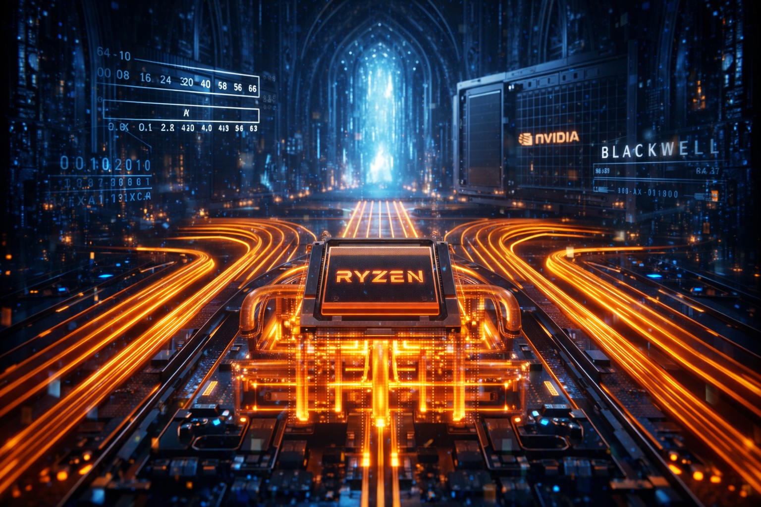
The 2026 Flagships: Zen 5 and Blackwell
We are currently witnessing a peak in silicon engineering with the AMD Ryzen 7 9800X3D and the NVIDIA RTX 5090.
1. The AMD Ryzen 7 9800X3D (Zen 5 Architecture)
AMD solved the “Heat Wall” of 3D V-Cache by inverting the chip. By placing the 96 MB of L3 cache underneath the cores, the CPU can touch the cooler directly. This allows it to hit 5.2 GHz while maintaining a massive memory pool, making it the fastest gaming CPU in history.
2. The NVIDIA RTX 5090 (Blackwell Architecture)
The RTX 5090 is a “Neural Titan.” With 32 GB of GDDR7 memory and 1.8 TB/s of bandwidth, it is designed not just to render frames, but to generate them using AI. It uses 5th Gen Tensor Cores to perform FP4 precision math, which is essential for the next generation of AI-driven graphics.
The Software Stack: From Python to Pulsing Silicon
The most miraculous part of computing is the translation layer. A modern developer might write a line of code in a “High-Level Language” like Python or JavaScript, which looks almost like English. However, the CPU is fundamentally “illiterate”—it only understands high and low voltages (1s and 0s).
1. The Hierarchy of Languages
- High-Level Languages (Python, Java, Rust): These are designed for human productivity. They use “Abstractions” to hide the complexity of the hardware. When you write
print("Hello"), the language handles the memory allocation, the font rendering, and the interface with the monitor automatically. - Assembly Language: This is the “Human-Readable” version of machine code. It has a 1:1 relationship with the CPU’s hardware. Instead of binary, it uses mnemonics like
MOV(Move),ADD(Add), andPUSH. This is where the Register Size we discussed earlier becomes vital; a programmer must specify if they are moving data into a 32-bit register (EAX) or a 64-bit register (RAX). - Machine Code (The Opcode): This is the final destination. It consists of hexadecimal strings like
48 89 D8. When these bits hit the CPU’s Instruction Decoder, they physically trigger the logic gates to perform a specific action.
2. Operating Systems and the Register State
The Operating System (OS), such as Windows 11 or macOS, acts as the “Traffic Controller” for the registers. Because a CPU has a limited number of physical registers (usually around 16–32 general-purpose ones in x86-64), the OS must perform a Context Switch thousands of times per second.
When you switch from your Web Browser to a Video Game, the OS must:
- Pause the Browser’s execution.
- Save the exact “State” of every 64-bit register into the RAM.
- Load the Game’s data into those same registers.
- Resume execution.
This happens so fast that it creates the illusion of simultaneous “Multitasking,” even though a single core is only doing one thing at any given microsecond.
The Multi-Threaded Symphony: SMT and Hyper-Threading
As we noted in the hardware section, we cannot simply increase clock speeds to 10 GHz. Instead, we use Concurrency. This is handled through two distinct methods: Hardware Threads and Software Threads.
1. Hyper-Threading (SMT): The Virtual Core
Developed by Intel (called Simultaneous Multithreading or SMT by AMD), this technology is a brilliant “efficiency hack.”
- A physical CPU core is often “waiting”—waiting for data from the L3 cache or waiting for a user to click a button.
- Hyper-Threading adds a second “Architectural State” (a second set of registers) to the same core.
- While Thread 1 is waiting for a “Cache Miss” from the RAM, the CPU instantly flips to Thread 2 to keep the execution units busy.
- This is why an 8-core Ryzen 7 9800X3D shows up as 16 Logical Processors in your Task Manager. It’s not two brains; it’s one brain with two sets of hands.
2. Software Threading and Parallelism
Modern software is written to be “Threaded.” A game might have one thread for Physics, one for Audio, and one for Networking.
- The Bottleneck: If a game is “Single-Thread Limited,” it means one specific task (like AI pathfinding) is so heavy that it’s maxing out one CPU core while the other 15 cores sit idle.
- The Solution: Modern languages like C++ and Rust allow developers to “spawn” hundreds of threads. The OS then distributes these across the available P-Cores and E-Cores, ensuring that background tasks like Discord or Antivirus don’t “stutter” your primary 64-bit gaming thread.
The Future: Neural Rendering and AI-Native Engines
The most exciting shift in computing is the move from Rasterization (calculating light) to Neural Rendering (predicting light).
1. AI-Driven Graphics
Technologies like DLSS 4 and Neural Radiance Fields (NeRFs) allow GPUs to render a low-resolution image and then “dream up” the high-resolution details. In 2026, many games render only 10% of the pixels traditionally—AI generates the other 90%. This allows for “Path Tracing,” where every single photon of light is simulated for photorealism.
2. AI-Native Game Engines
We are moving away from traditional engines like Unreal and Unity toward engines built on Emergent Logic.
- Generative Worlds: Instead of artists hand-placing every rock, AI models synthesize landscapes on the fly based on the game’s lore.
- Autonomous NPCs: Using engines like NVIDIA ACE, NPCs no longer have scripts. They have “personalities” and “memories,” allowing them to hold unscripted conversations and make their own decisions in the game world.
Conclusion
By combining these layers—Bits at the bottom, Registers in the middle, and High-Level Languages at the top—we create the modern experience. The NVIDIA RTX 5090 and AMD Ryzen 9800X3D are simply the most advanced “stages” ever built for this play.
The CPU manages the Logic (the “If/Then” of the OS), the GPU handles the Parallel Math (the pixels and AI), and the Operating System ensures the 64-bit instructions flow smoothly between them. We have moved from a world of simple “calculators” to a world of Neural Synthesis, where the machine isn’t just following instructions—it’s predicting the future of every frame on your screen.
As we push toward PCIe 6.0 and the eventual birth of 128-bit consumer systems, it will only grow more complex.